OV-C2-DD-THERMAL · v1.0 · released · 2026-07-17
| Doctype | Design Document |
|---|---|
| Doc id | OV-C2-DD-THERMAL |
| Product line | openvvvf |
| Applies to | chassis-size-2 |
| Version | 1.0 |
| Date | 2026-07-17 |
| Status | released |
| Description | IGBT and diode loss analysis, inverter efficiency, and heatsink/baseplate sizing for the Chassis Size 2 traction inverter. |
| Nav order | 230 |
| Normative refs | OV-C2-DD-INDEX, OV-C2-DD-DCLINK-THERMAL |
System Thermal Analysis
This document estimates the total heat dissipated into the heatsink by the 3-phase traction inverter power stage (3× Mitsubishi CM600DY-24T half-bridge IGBT modules plus the DC-link capacitor bank) and derives the heatsink thermal resistance required for continuous operation. It is the sizing input for the custom heatsink design.
Value marking convention used throughout:
- [DS] - value taken directly from the CM600DY-24T datasheet (Mitsubishi Electric, publication date December 2020); page/figure cited.
- [EST] - engineering estimate derived from datasheet curves (digitized) or standard scaling laws; not explicitly guaranteed by the datasheet.
- [ASM] - modeling assumption about the operating point.
Nomenclature
| Symbol | Meaning | Units |
|---|---|---|
| $A$ | Cross-sectional area (generic) | m² |
| $\cos \varphi$ | Load power factor | - |
| $d(\theta)$ | High-side switch duty cycle as a function of electrical angle | - |
| $E_{on}$ | IGBT turn-on switching energy per pulse | J |
| $E_{off}$ | IGBT turn-off switching energy per pulse | J |
| $E_{rr}$ | Free-wheeling diode reverse-recovery energy per pulse | J |
| $f_{sw}$ | PWM switching frequency | Hz |
| $i(\theta)$ | Instantaneous phase current as a function of electrical angle | A |
| $\hat{I}$ | Peak sinusoidal phase current ($\sqrt{2} \cdot I_{rms}$) | A |
| $I_C$ | IGBT collector DC current | A |
| $I_{CRM}$ | IGBT repetitive peak collector current | A |
| $I_E$ | Free-wheeling diode forward current | A |
| $I_{rms}$ | RMS phase current | A |
| $k$ | Thermal conductivity | W/(m·K) |
| $L$ | Length (thermal conduction path) | m |
| $m$ | Modulation index ($V_{ph,pk} / (V_{DC}/2)$) | - |
| $P_{cap}$ | DC-link capacitor bank heat load | W |
| $P_D$ | Free-wheeling diode conduction loss (per diode) | W |
| $P_{heat}$ | Total heat rejected to the heatsink | W |
| $P_{mod}$ | Heat dissipated per IGBT module | W |
| $P_{out}$ | Inverter output power | W |
| $P_Q$ | IGBT conduction loss (per IGBT) | W |
| $P_{semi}$ | Total semiconductor (IGBT + FWD) loss | W |
| $P_{sw,D}$ | Free-wheeling diode switching loss (per diode) | W |
| $P_{sw,Q}$ | IGBT switching loss (per IGBT) | W |
| $Q$ | Heat flow / power | W |
| $Q_G$ | IGBT gate charge | C |
| $Q_{rr}$ | Free-wheeling diode reverse-recovery charge | C |
| $r_{CE}$ | IGBT on-state resistance (chip + lead) | Ω |
| $r_D$ | Free-wheeling diode on-state resistance (chip + lead) | Ω |
| $R_G$ | External gate resistance | Ω |
| $R_{CC'+EE'}$ | Module internal lead resistance | Ω |
| $R_{th}$ | Thermal resistance | K/W |
| $R_{th(c-s)}$ | Module case-to-sink (baseplate-to-heatsink) thermal resistance | K/W |
| $R_{th(j-c)D}$ | Free-wheeling diode junction-to-case thermal resistance | K/W |
| $R_{th(j-c)Q}$ | IGBT junction-to-case thermal resistance | K/W |
| $R_{th(s-a)}$ | Heatsink surface-to-ambient thermal resistance | K/W |
| $t_{dt}$ | PWM dead time | s |
| $t_{rr}$ | Free-wheeling diode reverse-recovery time | s |
| $T_c$ | Module baseplate (case) temperature | °C |
| $T_j$ | Semiconductor junction temperature | °C |
| $T_{j,D}$ | Free-wheeling diode junction temperature | °C |
| $T_{j,Q}$ | IGBT junction temperature | °C |
| $T_{jmax}$ / $T_{jop}$ | Maximum / continuous operating junction temperature | °C |
| $T_s$ | Heatsink surface temperature under the module | °C |
| $T_{amb}$ | Ambient temperature | °C |
| $T_C$ | Module case temperature (datasheet reference) | °C |
| $T_{vj}$ | Virtual junction temperature | °C |
| $V_{CC}$ | DC-link voltage during switching-test conditions | V |
| $V_{CE(sat)}$ | IGBT collector-emitter saturation voltage | V |
| $V_{CES}$ | IGBT collector-emitter breakdown voltage | V |
| $V_{DC}$ | DC-link voltage | V |
| $V_{EC}$ | Free-wheeling diode forward voltage | V |
| $V_{EC0}$ | Free-wheeling diode threshold voltage (model fit) | V |
| $V_{CE0}$ | IGBT threshold voltage (model fit) | V |
| $V_{GE}$ | Gate-emitter drive voltage | V |
| $V_{ph,pk}$ | Peak phase voltage | V |
| $V_{ph,rms}$ | RMS phase voltage | V |
| $\Delta T$ | Temperature rise / difference | K or °C |
| $\eta$ | Inverter efficiency | - |
| $\lambda$ | Thermal conductivity (e.g., grease) | W/(m·K) |
| $\varphi$ | Current phase lag behind voltage (power-factor angle) | rad |
| $\theta$ | Electrical angle | rad |
References and system inputs
- CM600DY-24T datasheet, Mitsubishi Electric, December 2020 (600 A / 1200 V dual (half-bridge) IGBT module, 62 mm package).
OV-C2-DD-DCLINK-THERMAL- DC-link capacitor bank heat load of ≈40 W at rated ripple, rejected to the heatsink through the standoff/spreader-plate path.- Project README - power stage: 3× CM600DY-24T half-bridge modules (one per phase), SVPWM, default switching frequency 2 kHz (300 Hz – 16 kHz range), DC link 102–320 V (140 V nominal), 600 A class output. Gate drive +15 V / −9 V via onsemi NCV57100.
Datasheet parameters used (CM600DY-24T)
Ratings and electrical characteristics
| Parameter | Value | Conditions | Source | Mark |
|---|---|---|---|---|
| $V_{CES}$ | 1200 V | G–E shorted | Datasheet p.2, Maximum Ratings | [DS] |
| $I_C$ (DC) | 600 A | $T_C = 144 \ ^\circ\text{C}$ | Datasheet p.2 | [DS] |
| $I_{CRM}$ | 1200 A | repetitive pulse | Datasheet p.2 | [DS] |
| $V_{CE(sat)}$, chip | 1.55 V typ / 1.80 V max | $I_C = 600$ A, $V_{GE} = 15$ V, $T_{vj} = 25 \ ^\circ\text{C}$ | Datasheet p.2, Electrical Characteristics | [DS] |
| $V_{CE(sat)}$, chip | 1.75 V typ | $I_C = 600$ A, $V_{GE} = 15$ V, $T_{vj} = 125 \ ^\circ\text{C}$ | Datasheet p.2 | [DS] |
| $V_{CE(sat)}$, chip | 1.80 V typ | $I_C = 600$ A, $V_{GE} = 15$ V, $T_{vj} = 150 \ ^\circ\text{C}$ | Datasheet p.2 | [DS] |
| $V_{CE(sat)}$, terminal | 1.75 / 2.00 / 2.10 V typ (2.05 V max at 25 °C) | $I_C = 600$ A, 25 / 125 / 150 °C | Datasheet p.2 | [DS] |
| $V_{EC}$, chip (FWD) | 1.65 V typ (2.00 V max at 25 °C) | $I_E = 600$ A, 25 / 125 / 150 °C | Datasheet p.2 | [DS] |
| $V_{EC}$, terminal (FWD) | 1.85 / 2.00 / 2.00 V typ | $I_E = 600$ A, 25 / 125 / 150 °C | Datasheet p.2 | [DS] |
| $E_{on}$ | 56.6 mJ typ | $V_{CC} = 600$ V, $I_C = 600$ A, $V_{GE} = \pm 15$ V, $R_G = 1.0 \ \Omega$, $T_{vj} = 150 \ ^\circ\text{C}$, inductive load | Datasheet p.2 | [DS] |
| $E_{off}$ | 64.3 mJ typ | same conditions | Datasheet p.2 | [DS] |
| $E_{rr}$ | 38.2 mJ typ | same conditions, $I_E = 600$ A | Datasheet p.2 | [DS] |
| $Q_{rr}$ / $t_{rr}$ | 60 µC typ / 400 ns max | $V_{CC} = 600$ V, $I_E = 600$ A, $R_G = 1.0 \ \Omega$ | Datasheet p.2 | [DS] |
| $Q_G$ | 3.7 µC typ | $V_{CC} = 600$ V, $I_C = 600$ A, $V_{GE} = 15$ V | Datasheet p.2 | [DS] |
| $R_{CC'+EE'}$ (internal lead R) | 0.3 mΩ typ | per switch, $T_C = 25 \ ^\circ\text{C}$ | Datasheet p.2 | [DS] |
| Switching times | $t_{d(on)} \le 500$ ns, $t_r \le 200$ ns, $t_{d(off)} \le 600$ ns, $t_f \le 300$ ns | $V_{CC} = 600$ V, $I_C = 600$ A, $R_G = 1.0 \ \Omega$ | Datasheet p.2 | [DS] |
| $T_{jop}$ / $T_{jmax}$ | $-40 \dots +150 \ ^\circ\text{C}$ continuous / $175 \ ^\circ\text{C}$ instantaneous | - | Datasheet p.2 | [DS] |
| Recommended operating point | $V_{CC} = 600$ V typ (850 V max), $V_{GE(on)} = 15$ V, $R_G = 1.0$–$10 \ \Omega$ | - | Datasheet p.4 | [DS] |
Thermal resistances
| Parameter | Value | Per | Source | Mark |
|---|---|---|---|---|
| $R_{th(j-c)Q}$ | 24 K/kW max (= 0.024 K/W) | one inverter IGBT | Datasheet p.3, Thermal Resistance | [DS] |
| $R_{th(j-c)D}$ | 42 K/kW max (= 0.042 K/W) | one inverter FWD | Datasheet p.3 | [DS] |
| $R_{th(c-s)}$ | 13.3 K/kW typ (= 0.0133 K/W) | one module (grease $\lambda = 3.0$ W/(m·K), 50 µm) | Datasheet p.3, note 6 | [DS] |
Note: $R_{th(c-s)}$ is a typical value; no maximum is given. Grease ageing/pump-out (datasheet note 8) can raise it over life - covered by the heatsink margin policy in §6.
Device model parameters digitized from datasheet curves
Conduction models use the standard $V_0 + r \cdot I$ straight-line fit to the datasheet output/saturation curves at $T_{vj} = 125 \ ^\circ\text{C}$ (chip values), with the internal lead resistance $R_{CC'+EE'} = 0.3 \ \text{m}\Omega$ added because it dissipates heat inside the module:
| Model parameter | Value | Basis | Mark |
|---|---|---|---|
| $V_{CE0}$ | 1.15 V | Fit to $V_{CE(sat)}$ vs $I_C$ curve, chip, 125 °C (datasheet p.6, "Collector-Emitter Saturation Voltage Characteristics"); fit passes through (300 A, 1.45 V), (600 A, 1.75 V), (900 A, 2.05 V) | [EST] |
| $r_{CE}$ | 1.0 mΩ (+ 0.3 mΩ lead = 1.3 mΩ used) | same figure + p.2 lead resistance | [EST] |
| $V_{EC0}$ | 1.15 V | Fit to FWD forward curve, chip, 125 °C (datasheet p.6, "Free Wheeling Diode Forward Characteristics"); through (300 A, 1.38 V), (600 A, 1.65 V), (1200 A, 2.10 V) | [EST] |
| $r_D$ | 0.8 mΩ (+ 0.3 mΩ lead = 1.1 mΩ used) | same figure + p.2 lead resistance | [EST] |
Switching energy models (datasheet p.7, "Half-Bridge Switching Characteristics - switching energy vs collector/emitter current", $V_{CC} = 600$ V, $V_{GE} = \pm 15$ V, $R_G = 1.0 \ \Omega$; the solid $T_{vj} = 150 \ ^\circ\text{C}$ curves were used, anchored exactly at the p.2 table values at 600 A; the dashed 125 °C curves lie ≈5–10 % lower, so the 150 °C curves are conservative at the 125 °C operating point):
| $I_C$ / $I_E$ | $E_{on}$ | $E_{off}$ | $E_{rr}$ | Mark |
|---|---|---|---|---|
| 300 A | ≈ 30 mJ (fit 28 mJ) | ≈ 37 mJ | ≈ 31 mJ | [EST] |
| 600 A | 56.6 mJ | 64.3 mJ | 38.2 mJ | [DS] anchor |
| 850 A | ≈ 106 mJ | ≈ 94 mJ | ≈ 39 mJ | [EST] |
| 1200 A | ≈ 180 mJ | ≈ 130 mJ | ≈ 39 mJ | [EST] |
Piecewise-linear interpolation of these anchor points is used in the model. Digitization uncertainty is about ±5 % (line thickness / anti-aliasing). Note $E_{on}$ is markedly superlinear above 600 A, and $E_{rr}$ saturates above ≈700 A.
Scaling laws applied (not given in the datasheet):
- Voltage scaling: $E(V_{DC}) = E_{600\text{V}} \cdot (V_{DC} / 600 \ \text{V})$. Standard first-order scaling of switching energy with bus voltage. [EST]
- Temperature: 150 °C energy curves used at the 125 °C operating point (conservative). Conduction parameters at 125 °C. [EST]
- Gate conditions: datasheet energies are at $V_{GE} = \pm 15$ V and $R_G = 1.0 \ \Omega$; the inverter drives +15 V / −9 V. Energies are assumed equal; actual populated gate resistance must match the $R_G = 1.0 \ \Omega$ class or $E_{on}/E_{off}$ rise (datasheet p.7, $E$ vs $R_G$ figure: at $R_G = 10 \ \Omega$, $E_{on}$ roughly triples). [ASM]
Loss model and assumptions
Assumptions [ASM]
- 3 half-bridge modules, one per phase, symmetrical sharing.
- Modulation index $m = 1.0$, defined as $V_{ph,pk} = m \cdot V_{DC}/2$ (within the linear SVPWM range, which extends to $m = 1.15$ in this convention).
- Sinusoidal phase current $i(\theta) = \hat{I} \cdot \sin \theta$ with $\hat{I} = \sqrt{2} \cdot I_{rms}$.
- Load power factor $\cos \varphi = 0.8$ (traction motor at rated point).
- Junction operating point $T_j = 125 \ ^\circ\text{C}$ (continuous rating is 150 °C; 125 °C leaves margin).
- Switching frequency $f_{sw} = 2$ kHz (default); 16 kHz evaluated as worst case.
- Dead time (0.5–4 µs configurable): the extra FWD conduction during dead time adds ≈ $V_{EC} \cdot \langle i \rangle \cdot 2 \cdot t_{dt} \cdot f_{sw} \approx 7$ W per leg (~20 W total) at 600 A / 2 kHz / 2 µs - under 1 % of total heat, neglected.
- Gate-drive power ($Q_G \cdot \Delta V_{GE} \cdot f_{sw} \approx 0.2$ W per switch, ≈1 W total) is dissipated in the gate resistors/driver, not the module - excluded.
- $E_{on}$ as measured in the datasheet half-bridge circuit already contains the turn-on impact of the opposing diode's reverse recovery; $E_{rr}$ is counted once, in the diode (standard datasheet convention).
Formulas
High-side fundamental duty cycle of one leg (identical for SPWM and SVPWM to first order; third-harmonic injection does not change the fundamental average that sets the IGBT/FWD conduction split):
$$i(\theta) = \hat{I} \cdot \sin \theta \qquad \hat{I} = \sqrt{2} \cdot I_{rms}$$
$$d(\theta) = \frac{1}{2} \cdot \left(1 + m \cdot \sin(\theta - \varphi)\right)$$
Conduction loss per IGBT and per FWD (standard 2-level bridge result, integrating $v(i) \cdot i \cdot d(\theta)$ over the positive current half-wave):
$$P_Q = V_{CE0} \cdot \hat{I} \cdot \left(\frac{1}{2\pi} + \frac{m \cos \varphi}{8}\right) + r_{CE} \cdot \hat{I}^2 \cdot \left(\frac{1}{8} + \frac{m \cos \varphi}{3\pi}\right) \qquad \text{[per IGBT]}$$
$$P_D = V_{EC0} \cdot \hat{I} \cdot \left(\frac{1}{2\pi} - \frac{m \cos \varphi}{8}\right) + r_D \cdot \hat{I}^2 \cdot \left(\frac{1}{8} - \frac{m \cos \varphi}{3\pi}\right) \qquad \text{[per FWD]}$$
Switching loss, averaging the digitized energy curves over the sine half-wave and scaling with bus voltage:
$$P_{sw,Q} = f_{sw} \cdot \frac{V_{DC}}{600 \ \text{V}} \cdot \frac{1}{2\pi} \int_{0}^{\pi} \left[ E_{on}(i(\theta)) + E_{off}(i(\theta)) \right] d\theta \qquad \text{[per IGBT]}$$
$$P_{sw,D} = f_{sw} \cdot \frac{V_{DC}}{600 \ \text{V}} \cdot \frac{1}{2\pi} \int_{0}^{\pi} E_{rr}(i(\theta)) \, d\theta \qquad \text{[per FWD]}$$
Totals for the bridge (6 IGBTs + 6 FWDs) and the heatsink:
$$P_{semi} = 6 \cdot (P_Q + P_D + P_{sw,Q} + P_{sw,D})$$
$$P_{heat} = P_{semi} + P_{cap} \qquad P_{cap} = 40 \ \text{W}$$
$$P_{out} = 3 \cdot V_{ph,rms} \cdot I_{rms} \cdot \cos \varphi = \frac{3 \cdot m \cdot V_{DC} \cdot I_{rms} \cdot \cos \varphi}{2\sqrt{2}}$$
$$\eta = \frac{P_{out}}{P_{out} + P_{heat}}$$
Per-module dissipation (for the thermal chain):
$$P_{mod} = \frac{P_{semi}}{3}$$
Heat vs phase current
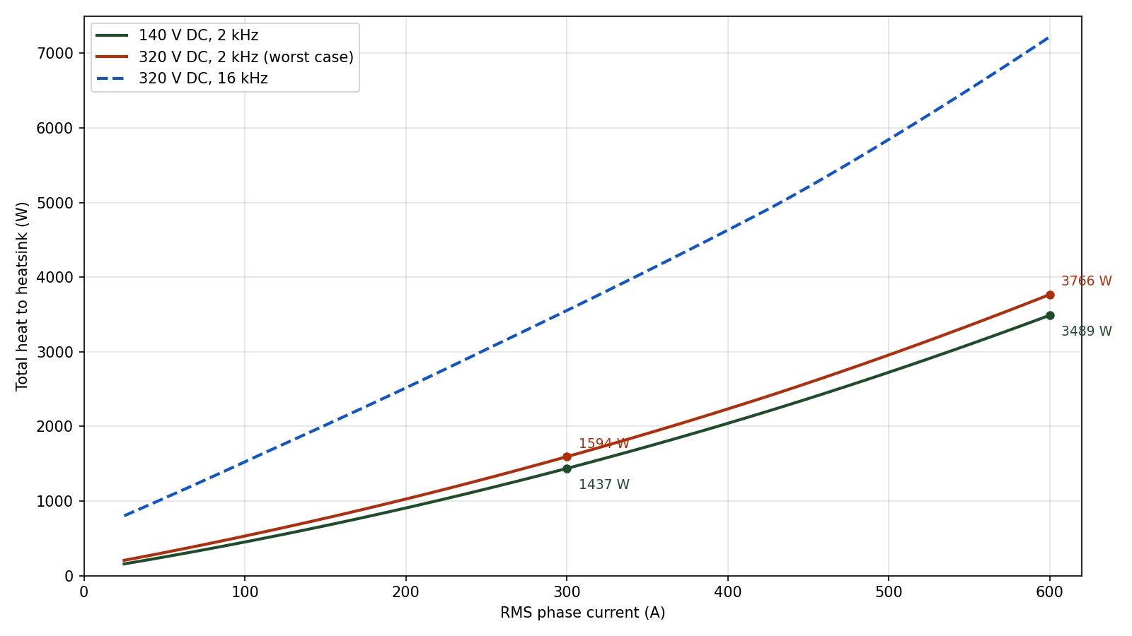
Total heat rejected to the heatsink (IGBT + FWD conduction and switching, plus 40 W capacitor heat), 2 kHz, $m = 1.0$, $\cos \varphi = 0.8$:
| $I_{phase}$ (A rms) | IGBT cond., 6× (W) | FWD cond., 6× (W) | Switching, 6× @140 V (W) | Caps (W) | Total @140 V / 2 kHz (W) | Total @320 V / 2 kHz (W) | Total @320 V / 16 kHz (W) |
|---|---|---|---|---|---|---|---|
| 50 | 135 | 30 | 46 | 40 | 250 | 309 | 1038 |
| 100 | 286 | 63 | 62 | 40 | 451 | 531 | 1525 |
| 150 | 453 | 99 | 78 | 40 | 669 | 770 | 2016 |
| 200 | 637 | 137 | 93 | 40 | 906 | 1026 | 2516 |
| 250 | 837 | 177 | 108 | 40 | 1162 | 1301 | 3032 |
| 300 | 1053 | 221 | 122 | 40 | 1437 | 1594 | 3552 |
| 350 | 1286 | 267 | 136 | 40 | 1729 | 1904 | 4084 |
| 400 | 1535 | 316 | 150 | 40 | 2041 | 2233 | 4630 |
| 450 | 1801 | 367 | 164 | 40 | 2372 | 2583 | 5208 |
| 500 | 2083 | 421 | 180 | 40 | 2724 | 2957 | 5845 |
| 550 | 2381 | 478 | 198 | 40 | 3097 | 3351 | 6517 |
| 600 | 2696 | 537 | 216 | 40 | 3489 | 3766 | 7219 |
Conduction dominates at 2 kHz (switching is only ≈6 % of semiconductor loss at 140 V / 600 A because the energies scale with $V_{DC}/600 \ \text{V}$). At 320 V / 16 kHz switching becomes dominant (≈3.9 kW of the 7.2 kW at 600 A).
Loss breakdown at the two design currents (140 V, 2 kHz):
| Quantity | 300 A rms | 600 A rms |
|---|---|---|
| Per-IGBT conduction | 176 W | 449 W |
| Per-FWD conduction | 37 W | 89 W |
| Per-IGBT switching | 14 W | 28 W |
| Per-FWD switching ($E_{rr}$) | 7 W | 8 W |
| Per module ($P_{semi}/3$) | 466 W | 1150 W |
| Semiconductor total | 1397 W | 3449 W |
| Total to heatsink (incl. 40 W caps) | 1437 W | 3489 W |
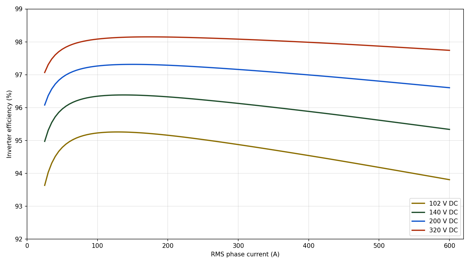
Inverter efficiency vs phase current
$$\eta = \frac{P_{out}}{P_{out} + P_{heat}} \quad \text{at } m = 1.0, \ \cos \varphi = 0.8, \ 2 \ \text{kHz}$$
including the 40 W capacitor heat.
$$P_{out} = \frac{3 \cdot m \cdot V_{DC} \cdot I_{rms} \cdot \cos \varphi}{2\sqrt{2}}$$
i.e., each bus voltage runs at its rated fundamental output voltage ($P_{out}$ at 600 A: 52 kW @102 V, 71 kW @140 V, 102 kW @200 V, 163 kW @320 V).
| $I_{phase}$ (A rms) | $\eta$ @102 V (%) | $\eta$ @140 V (%) | $\eta$ @200 V (%) | $\eta$ @320 V (%) |
|---|---|---|---|---|
| 50 | 94.8 | 96.0 | 96.9 | 97.8 |
| 100 | 95.2 | 96.3 | 97.3 | 98.1 |
| 150 | 95.2 | 96.4 | 97.3 | 98.1 |
| 200 | 95.2 | 96.3 | 97.3 | 98.1 |
| 250 | 95.0 | 96.2 | 97.2 | 98.1 |
| 300 | 94.9 | 96.1 | 97.2 | 98.1 |
| 350 | 94.7 | 96.0 | 97.1 | 98.0 |
| 400 | 94.5 | 95.9 | 97.0 | 98.0 |
| 450 | 94.4 | 95.8 | 96.9 | 97.9 |
| 500 | 94.2 | 95.6 | 96.8 | 97.9 |
| 550 | 94.0 | 95.5 | 96.7 | 97.8 |
| 600 | 93.8 | 95.3 | 96.6 | 97.7 |
At the 140 V nominal bus the efficiency peaks at ≈96.4 % around 150–200 A and falls to 95.3 % at 600 A, because conduction loss grows faster than output power (the $r \cdot I^2$ term). Higher bus voltages are more efficient at the same current because conduction loss is unchanged while output power scales with $V_{DC}$.
Heatsink sizing
Thermal chain
Steady-state 1-D chain from junction to ambient for the hottest IGBT of a module:
$$T_s = T_{amb} + P_{heat} \cdot R_{th(s-a)}$$
$$T_c = T_s + P_{mod} \cdot R_{th(c-s)}$$
$$T_{j,Q} = T_c + (P_Q + P_{sw,Q}) \cdot R_{th(j-c)Q}$$
$$T_{j,D} = T_c + (P_D + P_{sw,D}) \cdot R_{th(j-c)D}$$
- $R_{th(c-s)} = 13.3$ K/kW typ per module (thermal grease) [DS p.3]
- $R_{th(j-c)Q} = 24$ K/kW max, $R_{th(j-c)D} = 42$ K/kW max [DS p.3]
- Design limits: module baseplate $T_c \le 85 \ ^\circ\text{C}$ at $T_{amb} = 40 \ ^\circ\text{C}$; junction target $T_j \le 125 \ ^\circ\text{C}$ with margin (continuous rating 150 °C [DS]). The 85 °C baseplate limit is also consistent with the SWAD NTC monitor (100 °C hard cap on the module-sited NTC) and with the DC-link spreader plate, which reaches ≈80 °C at a 40 °C heatsink base under its 40 W load (
OV-C2-DD-DCLINK-THERMAL).
Required heatsink thermal resistance
Worst case is 320 V bus (highest switching loss); 140 V nominal shown for reference, 16 kHz as the upper switching bound.
| Operating point | $P_{heat}$ (W) | $P_{mod}$ (W) | $\Delta T_{(c-s)}$ (K) | Max $T_s$ (°C) | Required $R_{th(s-a)}$ | $T_{j,Q}$ check | $T_{j,D}$ check |
|---|---|---|---|---|---|---|---|
| 300 A / 320 V / 2 kHz | 1594 | 518 | 6.9 | 78.1 | ≤ 0.0239 K/W | 90 °C ✓ | 87 °C ✓ |
| 600 A / 320 V / 2 kHz (design point) | 3766 | 1242 | 16.5 | 68.5 | ≤ 0.0076 K/W | 97 °C ✓ | 90 °C ✓ |
| 600 A / 140 V / 2 kHz (reference) | 3489 | 1150 | 15.3 | 69.7 | ≤ 0.0085 K/W | 96 °C ✓ | 89 °C ✓ |
| 600 A / 320 V / 16 kHz (reference) | 7219 | 2393 | 31.8 | 53.2 | ≤ 0.0018 K/W | 108 °C ✓ | 95 °C ✓ |
Guidance
- Continuous 600 A (design point): $R_{th(s-a)} \le 0.0076$ K/W (7.6 mK/W) for the whole three-module heatsink assembly, 40 °C ambient. With ≥25 % engineering margin (grease ageing, digitization/typ-value uncertainty, module-to-module variation, fouling), the design target is ≈ 0.006 K/W or better. This is outside natural-convection territory (a very large natural-convection sink is ≈0.1–0.5 K/W); it requires a large forced-air heatsink or a liquid cold plate.
- Continuous 300 A: $R_{th(s-a)} \le 0.024$ K/W - achievable with a moderate forced-air extrusion.
- The junction rise is small at the design point ($T_{j,Q} \approx 97 \ ^\circ\text{C}$ at $T_c = 85 \ ^\circ\text{C}$, ≈28 °C margin to the 125 °C target) because $R_{th(j-c)}$ is only 24 K/kW; the baseplate ≤ 85 °C constraint, not the junction, sizes the heatsink. Per-switch dissipation of ≈520 W at 600 A / 320 V / 2 kHz is also well inside the module's 6250 W total dissipation rating (datasheet p.2).
- 16 kHz operation at high current is impractical with air cooling (≤1.8 mK/W needed at 600 A) and marginal even with liquid cooling; treat 16 kHz as a reduced-current mode (see §7).
- Mounting: thermal grease per datasheet note 6 ($\lambda = 3.0$ W/(m·K), 50 µm), M6 mounting torque 3.5–4.5 N·m (datasheet p.3), baseplate flatness ≤ 200 µm on the centerlines. Verify the three modules are placed so each sees comparable sink temperature.
Sensitivity and notes
- 16 kHz switching: switching loss scales linearly with $f_{sw}$ (×8 vs 2 kHz). At 600 A / 320 V total heat rises from 3.8 kW to 7.2 kW and the heatsink requirement tightens from 7.6 to 1.8 mK/W. At 300 A / 320 V / 16 kHz the total is 3.55 kW and the requirement is $R_{th(s-a)} \le 8.3$ mK/W (same chain) - still forced-air/liquid territory. Recommend keeping 16 kHz for light-load/low-noise operation only.
- Lower power factor: total heat is nearly unchanged (the IGBT $V_0$ term falls while the FWD share rises; at $\cos \varphi = 0.5$, 600 A / 140 V / 2 kHz, $P_{heat} \approx 3.46$ kW vs 3.49 kW at $\cos \varphi = 0.8$), but output power falls proportionally with $\cos \varphi$, so efficiency drops (≈92.8 % at $\cos \varphi = 0.5$, 600 A / 140 V) and heat per kW delivered rises. Regenerative braking ($\cos \varphi < 0$) shifts loss toward the FWDs - $R_{th(j-c)D} = 42$ K/kW keeps the diode junction ≈5 °C cooler than the IGBT at rated point, so this is not binding.
- Typical vs maximum device values: conduction uses typical chip $V_{CE(sat)}/V_{EC}$; the max terminal values are ≈10–15 % higher, and $R_{th(c-s)}$ is a typical (not max) value. The ≥25 % heatsink margin policy covers this.
- 600 A RMS operation: at 600 A RMS the sine peak is 848 A, above the module's 600 A DC rating (at $T_C = 144 \ ^\circ\text{C}$) but within the 1200 A repetitive pulse rating. Continuous 600 A RMS is the inverter's design target (README), with full-load dyno/thermal validation still pending - treat the 600 A column as the sizing bound, not a validated continuous rating.
- Gate resistance: all switching energies assume the datasheet $R_G = 1.0 \ \Omega$ condition. If the populated gate resistance is larger, $E_{on}/E_{off}$ increase substantially (≈3× at 10 Ω for $E_{on}$, datasheet p.7) - re-run this analysis if the gate design deviates.
- Low-current extrapolation: below ≈100 A the $E_{rr}/E_{off}$ curve extrapolation carries the constant offsets ($E_{off} \approx 8.7$ mJ, $E_{rr} \approx 12$ mJ); the resulting low-current, high-frequency numbers (e.g., 50 A / 16 kHz) are the least accurate in this document, ±15 %.
- Not modeled: stray-inductance overshoot losses, module NTC self-heating, busbar/terminal ohmic heating into the heatsink (small vs 3.5 kW), and heatsink thermal spreading between modules (left to the heatsink detailed design). Ambient 40 °C is assumed at the heatsink inlet; inside a sealed chassis, derate accordingly.
- Firmware tie-in: the real-time loss estimator uses the same model structure ($V_{ce0}/R_{ce}$ conduction + $E_{on}/E_{off}$ curves + $R_{th}$ chain); the parameters in §2.3 are the recommended calibration set for it.
This is a design estimate for heatsink sizing, to be validated by test on the assembled inverter.